
| Home | S-100 Boards | History | New Boards | Software | Boards For Sale |
| Forum | Other Web Sites | Quiz | Index |
 |
 |
.jpg)
| 1 |
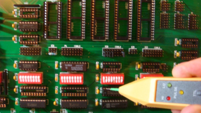
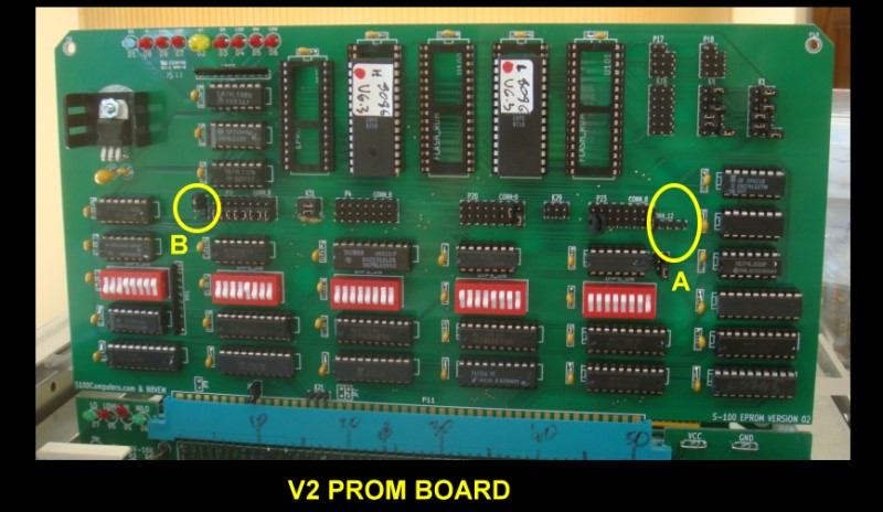
Connect
BOARD_WAIT to pin 7 of U17 (instead of pin 9). |
|
| 2 |
Have a jumper at pin 8 of U2C
that can go to either pin 9 of U2c or pin 11 of U124B, 16CSB*
(this eliminates wait states if RAM is used). |
|
| 3 |
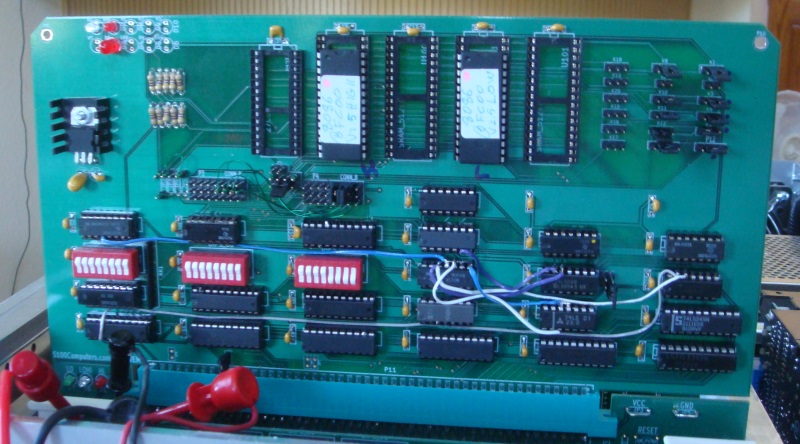
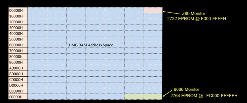
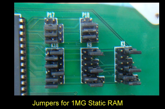
Bring out A16, A17, A18 and A19 as extra jumper contacts at P22.
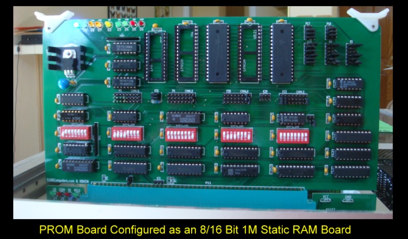
(Jumpers A below) This allows an EPROM at FC000H if 1MG static RAM is present at 0000H. For the V1 board, we needed wires from P1 to p24. |
This page was last modified on 09/26/2011